Friday, 22 April 2016

Password Based Circuit Breaker

Contents [show]
Nowadays, electrical accidents to the line man are increasing, while repairing the electrical lines due to the lack of communication between the electrical substation and maintenance staff. This project gives a solution to this problem to ensure line man safety. In this proposed system the control (ON/OFF) of the electrical lines lies with line man.
This project is arranged in such a way that maintenance staff or line man has to enter the password to ON/OFF the electrical line. Now if there is any fault in electrical line then line man will switch off the power supply to the line by entering password and comfortably repair the electrical line, and after coming to the substation line man switch on the supply to the particular line by entering the password. Before going to know about this circuit, also read the interesting post: Password based door locking system.
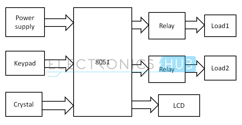
Block Diagram:

Block Diagram of Password Based Circuit Breaker

Principle:

The main component in the circuit is 8051 microcontroller. In this project 4×3 keypad is used to enter the password. The password which is entered is compared with the predefined password. If entered password is correct then the corresponding electrical line is turned ON or OFF. In this project a separate password is provided to each electrical line. Activation and deactivation of the line (circuit breaker) is indicated by the load.
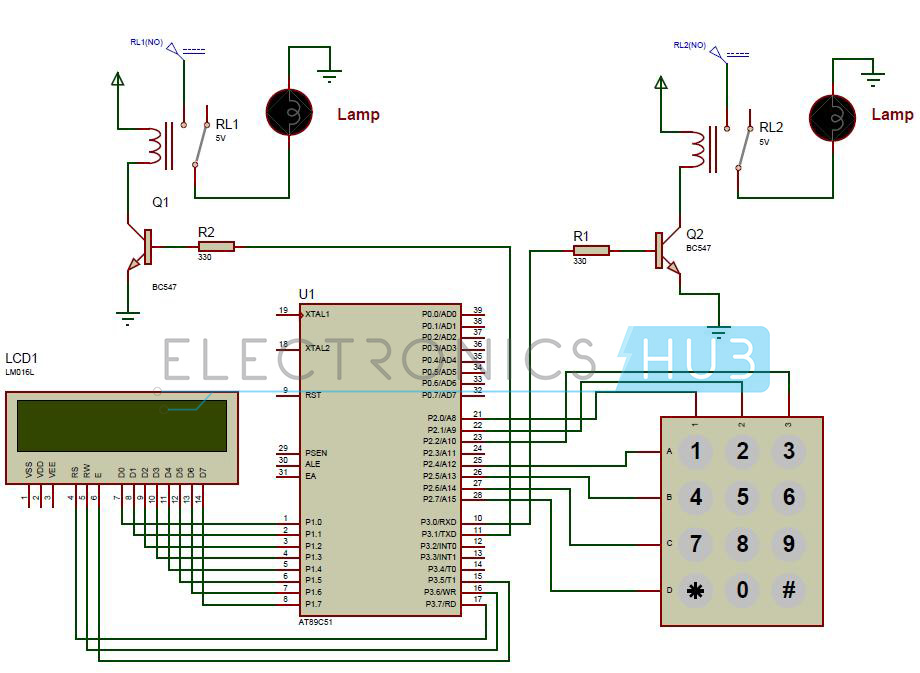
Circuit Diagram:

Password Based Circuit Breaker Circuit Diagram
Add caption
Password Based Circuit Breaker Circuit Diagram
Hardware Requirements:
  • at89c51 controller
  • 8051 programming board
  • Programming cable
  • DC battery or 12V,1A adaptor
  • 4×3 keypad
  • 16×2 LCD
  • 5V Relays – 2
  • Lamps – 2
  •  BC 547 Transistors – 2
  • 330 ohm resistors (1/4 watt) – 2
  • connecting wires
Software Requirements:
  • Keil compiler
  • Flash magic
  • Proteus

Circuit Design:

The above circuit consists of 8051 series controller, 4×3 keypad, LCD, relays and two loads. LCD data pins are connected to PORT1 and control pins RS, RW, EN pins are connected P3.7, P3.6 and P3.5 respectively. Here LCD is used to display the information. Keypad is connected to PORT2 of the controller. Using this keypad we need to enter the password. Lamps are connected to P3.0 and P3.1 through the relays. These are used to indicate circuit breaker state.
In this project we have used bc547 transistors to drive the relays. AC load should be connected to COM and NO (Normally open) pins. 5V relays are used to drive the AC loads.

Algorithm:

  1. Initially declare the PORT1 to LCD data pins and control pins to P3.5, P3.6 and P3.7 and declare PORT2 to keypad. And use P3.0, P3.1 to loads.
  2. Initially display enter password on LCD.
  3. Now read the five digit password from the user.
  4. Compare the entered password with stored password.
  5. If correct then ON or OFF the particular load and display line or load status on LCD.
  6. If the password is wrong then display PWD IS WRONG on LCD.
  7. After some delay again ask to enter password

If you need Source code to contact this address
Saqlain6050@gmail.com
Ph# +923089223448

Thursday, 21 April 2016

Simple Adjustable Timer Circuit
with 555 ICSimple Adjustable Timer Circuit
with 555
Circuit Diagram


Using simple 555 timer we can design an
adjustable timer switch. This circuit is flexible to
adjust required time.
Circuit Diagram
Components
555 timer
Electrolytic capacitor – 470 uf
ceramic capacitor – 0.1nF
Resistors
120k ohm
10k ohm
Relay -12v
Push button
Working
Here 555 timer is operated in monostable mode .
When the trigger input is applied,555 timer
produces a pulse. This pulse width depends on R
and c values.
The above proposed circuit is a 1-10 minute
timer.When Pot is minimum it gives 1 minute
delay,where maximum value of pot can produce
10 minutes.
Time period can be calculated using formula
T=(R1+R2)*C1.seconds
When Pot is maximum R is 120K+1.1M ≈ 1.2M
(approximately) and C1=470uf
T= 1.2M*470uF = 620 seconds≈10 minutes.This
is the maximum time.
For minimum time place the pot in least
position.Then R= 120k
Hence time T=120k*470uf=6 2 seconds~1
minute (approximately).
A 12v relay is used to drive the ac load
connected at the output.
Thus relay will be on for required amount of time
set by the user using pot and then it is switched
of automatically.
This circuit is used in such applications where
the load is switched on for sometime and is off
for rest of the time.
Note
To prevent 555 timer from flyback current in the
relay use a diode before the relay.
Some 555 versions may get damaged because of
this.

Friday, 15 April 2016

FM Radio Transmitter

Here we are building a wireless FM transmitter which uses RF communication to transmit the medium or low power FM signal. The maximum range of transmission is around 2 km.

FM Transmitter Circuit Principle:

FM transmission is done by the process of audio pre amplification, modulation and then transmission. Here we have adapted the same formula by first amplifying the audio signal, generating a carrier signal using an oscillating and then modulating the carrier signal with the amplified audio signal. The amplification is done by an amplifier, whereas the modulation and carrier signal generation is done by an variable frequency oscillator circuit. The frequency is set at anywhere between the FM frequency range from 88MHz to 108MHz. The power of the FM signal from the oscillator is then amplified using a power amplifier to produce a low impedance output, matching that with the antenna.

Circuit Diagram of 2 km FM Transmitter Circuit:

Circuit Diagram of FM Transmitter
FM Transmitter Circuit Diagram – ElectronicsHub.Org
Circuit Components:
COMPONENT NAME
VALUE
R1
18K
R2
22K
R3
90K
R4
5K
R5
540 Ohms
R6
9K
R7
40K
R8
1K
R9
20K
C1
5uF, Electrolyte
C2
47uF, Electrolyte
C3
0.01uF, Electrolyte
C4
15uF, Electrolyte
C5
0.01uF, Ceramic
C6
20pF, Variable Capacitor
C7
10pF, Ceramic
C8
20pF, Variable Capacitor
L1, L2
0.2uH
Antenna
30 Inches Long Wire or Telescopic Antenna
V1
9V Battery
Audio Input
Microphone

FM Transmitter Circuit Design:

Design of Audio Pre-amplifier:
Here we are designing a simple single stage common emitter amplifier as the pre-amplifier.
a) Selection of Vcc: Here we have selected the NPN Bipolar Junction Transistor, BC109. Since VCEO for this transistor is around 40V, we choose a much lesser Vcc, of about 9V.
b) Selection of Load Resistor, R4: To calculate the value of load resistor, we first need to calculate the quiescent collector current. Let us assume this value to be about 1mA. The collector voltage needs to be about half of Vcc. This gives the value of load resistor, R4 as :  Vc/Iq = 4.5K. We select a 5K resistor for better operation.
c) Selection of Voltage Divider Resistors R2 and R3: To calculate the value of the voltage divider resistors, we need to calculate the bias current as well the voltage across the resistors. The bias current is approximated to be 10 times the base current. Now base current, Ib is equal to the collector current divided by the current gain, hfe. This gives the value of Ib to be 0.008mA. The bias current is thus 0.08mA.
The voltage across the base, Vb is assumed to be 0.7V more than the emitter voltage Ve. Now assume the emitter voltage to be 12% of Vcc, i.e. 1.08V. This gives Vb to be 1.78V.
Thus, R2 = Vb/Ibias = 22.25K. Here we select a 22K resistor.
R3= (Vcc-Vb/Ibias = 90.1K. Here we select a 90K resistor.
d) Selection of Emitter Resistor R5: The value of R5 is given by Ve/Ie, where Ie is the emitter current and is approximately equal to the collector current. This gives R5 = (Ve/Ie) = 540 Ohms. Here we select a 500Ohms resistor.  It serves the purpose of bypassing the emitter current.
e) Selection of coupling capacitor, C1: Here this capacitor serves the purpose of modulating the current going through the transistor. A large value indicates low frequency (bass), whereas a lesser value increases treble (higher frequency). Here we select a value of 5 uF.
f) Selection of Microphone Resistor R1: The purpose of this resistor is to limit the current through the microphone, which should be less than the maximum current a microphone can handle. Let us assume the current through microphone to be 0.4mA. This gives the value of Rm = (Vcc-Vb)/0.4 = 18.05K. Here we select a 18K resistor.
g) Selection of Bypass Capacitor, C4: Here we select an electrolyte capacitor of 15 uF, which bypasses the DC signal.
Design of Oscillator Circuit:
a) Selection of tank circuit components – L1 and C6: We know the frequency of oscillations is given by
f = 1/(2∏√LC)
Here we require a frequency between 88 MHz to 100 MHz. Let us select a 0.2uH inductor. This gives value of C6 to be around 12pF. Here we select a variable capacitor in the range 5 to 20pF.
b) Selection of Tank Capacitor, C9: This capacitor serves the purpose of keeping the tank circuit to vibrate. Since here we are using BJT 2N222, we prefer the value of C9 between 4 to 10 pF. Let us select a 5 pF capacitor.
c) Selection of bias resistors R6 and R7: Using the same method for calculation of bias resistors, as in the preamplifier design, we select the values of bias resistors R6 and R7 to be 9 K and 40 K respectively.
d) Selection of coupling capacitor, C3: Here we select electrolyte capacitors of about 0.01 uF as the coupling capacitor.
e) Selection of emitter resistor, R8: Using the same calculations as for the amplifier circuit, we get the value of emitter resistor to be around 1K.
Design of Power Amplifier Circuit:
Since we require a low power output, we prefer using a class A power amplifier with LC tank circuit at the output. The values of the tank circuit components are same as that in oscillator circuit. Here we select the biasing resistor to be about 20 K and coupling capacitor of about 10 pF.
Selection of Antenna:
Since the range is about 2 km, we can prepare an antenna using a stick antenna or a wire of 30 inches approximately which would be about 1/4th of the transmitting wavelength.

Theory Behind FM Transmitter Circuit:

Audio signal from the microphone is very low level signal, of the order of mill volts. This extremely small voltage needs to be first amplified. A common emitter configuration of a bipolar transistor, biased to operate in class A region, produces an amplified inverted signal.
Another important aspect of this circuit is the colpitt oscillator circuit. This is a LC oscillator where energy moves back and forth between the inductor and capacitor forming oscillations. It is mainly used for RF application.
When this oscillator is given a voltage input, the output signal is a mixture of the input signal and the oscillating output signal, producing a modulated signal.  In other words, the frequency of the oscillator generated circuit varies with the application of an input signal, producing a frequency modulated signal.

How to Operate FM Transmitter Circuit?

Audio input from the microphone or any other device is first amplified using the common emitter configuration of BC109. This amplified signal is then given to the oscillator circuit through the coupling capacitor.  The oscillator circuit generates a signal with a frequency determined by the value of the variable capacitor. The output signal from the emitter of the transistor is coupled to the input of the power amplifier transistor using the coupling capacitor. As this signal is amplified, the variable capacitor in the power amplifier section tends to maintain an output matching with that of the oscillator. The amplified RF signal is then transmitted using antenna.
Applications of FM Transmitter Circuit:
This circuit can be used at any place to transmit audio signals using FM transmission, especially at institutions and organizations.
Limitations:
This circuit is for educational purposes and may require more practical approach.
  • Source:_  ElectronicsHub 
  • Thanks..For Supporting us
  • For Any Help on Projects or Other circuits.
Contact.No:+923089223448